

February
2022
Note: This article was created to sit alongside training that was run at a conference recently. The article can be used in its own right, but you may need to acquire some components and tools to follow along.
The Hardware Workshop at Home Edition
Ever wondered where to begin on a target that no one has ever looked at before? Once you get down to the hardware almost every target looks the same! Follow along with our “Hardware Workshop from Home” and Joel will show you how to speak the hardware language, and gain access to debugging features that are common to almost all kinds of device.
Prerequisites
Software List
- OpenOCD
- ARM Toolchain (Specifically: arm-none-eabi-gdb)
- STM32CubeIDE
- SigRok
- Putty
- Zadig Driver Installer (Windows Only)
Hardware List
Wiring Guide
This lab is aimed at people who want to be able to attack devices at the hardware level but may not have much experience with electronics or low-level communication protocols. It is intended to be an introduction to those who are just starting their journey into cyber security or who may have some experience attacking software and wish to start applying those skills to physical hardware but may not know where to start. When attacking hardware, our goals are usually a little different to when we are attacking something like a web application or piece of software. Usually, our main reason for attacking the hardware is to find a way to extract the firmware so that it can be reverse engineered. Another reason may be to try and extract secrets from the device, such as firmware signing keys allowing us to run our own custom firmware later.
If you do not have the challenge code flashed to your device, you can download the project files at the bottom of the page.
Reading PCBs
We will start out with what I normally refer to as “reading a PCB”. PCB stands for “Printed Circuit Board” and it’s the internal part of the device which you will be presented with when you first take a device apart. It is the main component to which all the electronics are attached.
The first step is a visual inspection of the PCB. With this step, we will usually be able to infer a high level, mental, flow diagram giving us a basic understanding of what the main components of the device are, and what is likely to be interesting to attack. One of our main goals at this point is also to determine which parts of the PCB are not interesting to us as attackers so we do not waste too much time reverse engineering or attacking a part of the device which is not going to yield anything useful.
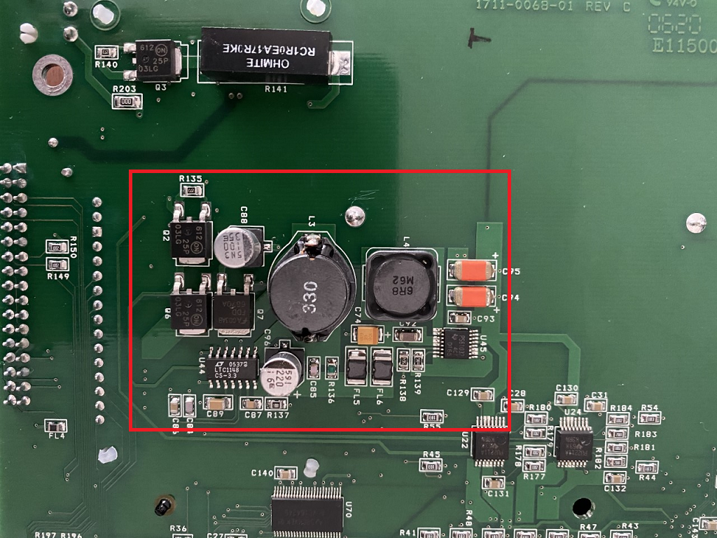
Power Management
The images above show a PCB taken from a device with several sections highlighted. Usually, the first area we want to identify is the power handling section of the device. The device will need power from somewhere, whether it be from a 12V power jack or a battery, and the area of the PCB near where the power is connected will contain the components used to step the voltage down to something which is more suitable for the main CPU or microcontroller and will usually include some filtering to ensure that the main processing components receive stable, clean power. This filtering can usually be easily identified by a group of filtering capacitors (usually large cylindrical components) near where the power enters the device.
Once the power handling section of the PCB has been identified, we need to find what voltage the main processing devices use since this will determine what voltage our tools need to be. The majority of electronic devices on the market today will use 3.3V or 5V with 3.3V being the most common. The easiest way to determine what voltage we need to use is to identify the voltage regulators which are used to step down (or in the case of some battery powered devices, step up) the voltage from the input voltage and regulate it at a steady 3.3 or 5 Volts. The most common voltage regulator you will come across are usually small rectangular devices with 3 pins on one side and a large tab on the other side. If you identify a component that looks like this then a simple google search for it’s datasheet should tell you whether it is a 5V or 3.3V regulator. In the case of adjustable/variable output regulators, the datasheet will give you the pinout of the device and you can use a multimeter to measure the voltage between the output and GND (ground) pins.
Once we have determined what voltage the device operates at, we can largely ignore the power handling section of the PCB.
I/O Filtering
Most devices are going to have some kind of input and output connectivity, for example, a Wi-Fi router will usually have ethernet connections and possibly a connection for an ADSL line. Connections like this, where it is expected that end users will be attaching and detaching cables and other devices, are likely to have input protection and input filtering circuitry near to the physical port. For our purposes, we can ignore these components as well since they won’t provide us with anything useful to attack.
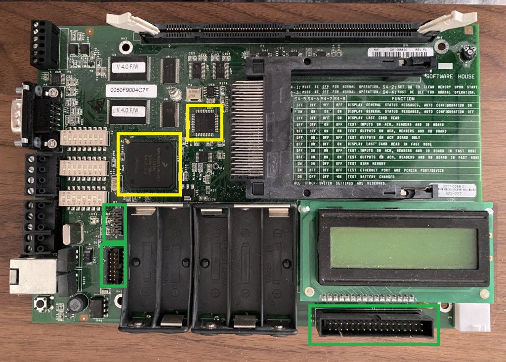
Main Processing
The next section we want to identify, which will be useful to us as attackers, are the main processing components, these are highlighted in yellow above. Usually, there will only be one and it is likely to be the largest chip, most likely with no pins visible. The reason there will likely not be any pins visible is because many modern processors or System-on-Chips (SoCs) use a Ball Grid Array (BGA) package which means the connections to the PCB is a grid of solder joints on the underside of the device. Once you have identified potential candidate devices for the main processing devices it is worth searching the internet to try and find their datasheets. This can be done by simply entering the part number into google but be aware that some manufacturers only release the datasheets for certain devices to developers under NDA so they may not be public.
Once you’ve identified the main processing components and read through their datasheets, then the next thing we want to know is where its firmware is stored. In your search for datasheets, it’s possible that you identified some eMMC flash devices or other flash chips which are likely to store the firmware, if not, the firmware may be stored in the device itself (usually this is only the case if the firmware is fairly simple since the devices themselves don’t usually have much storage). Flash chips themselves are usually BGA packages as well and will be located near to the main CPU. On some simpler devices they may just use a small 8 pin flash chip, these can usually only store about 8MB but they’re cheap making them ideal for situations where the firmware doesn’t need to be very complicated.
Connectivity Headers
At this point, you probably have a bit of an understanding about how the pieces fit together and what each section of the PCB does, and what parts of it you’ll be wanting to attack, usually, the main processor and/or the flash. What we need is a way to communicate with the device, the next section will focus on common communication protocols but for now we have one more thing left to identify which is the physical connection headers which we will use to connect our tools.
Looking around the PCB, you will want to find any rows of holes or in some cases, if you’re lucky, rows of pins. You will be looking for a single row of 4 pins and possibly 2 rows of 3, 5, or 10 pins. This is not, however, a hard and fast rule so look for any populated or unpopulated headers. If you are really unlucky there may not be any headers at all, instead there may only be small circular pads in which case you will need to solder wires on to these pads and try to reverse engineer what they are connected to. This process is beyond the scope of this blog post but if you do end up soldering wires to the pads, I can recommend using thin silicon wire because it is much less likely to tear the pad from the PCB when you are moving things around.
If you find a single row of 4 (or maybe just 3) pins, it is likely this is a Serial connection and could give you a console on the device. If you find 2 rows of pins (usually 3 or 5) then it is possible that you have found a JTAG header and may be able to debug the device, read the contents of Flash or otherwise interact with the hardware at a very low level.
Communication Protocols
Universal (Synchronous) Asynchronous Receive/Transmit
U(S)ART, more commonly known as Serial, is simple communication protocol used mainly to provide a human interface to a hardware device, i.e., to provide technicians or end users with a console on the device which can be used for configuration when there is no screen, or the developers want to allow for extra debugging capabilities not intended for normal end users.
The physical connections required for serial communications are fairly simple. Each device has a transmit and receive (TX and RX) and the connection is made from one device’s TX to the other device’s RX. You will also need to connect the two device’s grounds together, usually there is a pin on the header connected to GND so make sure these are connected together as well otherwise you will get garbage data.
Serial communications are almost always asynchronous because it makes the connections simpler. However, this means that the two devices need to agree on some parameters beforehand so that the communication will work. The parameters which need to be configured are:
- Baud rate
- Number of data bits
- Number of parity bits
- Number of stop bits
The baud rate in any communication system refers to the symbol rate of the protocol, in a binary system such as this, the baud rate is equal to the bit rate. The lowest baud rate you will likely come across is 9600 baud but this is usually only when following hobbyist tutorials on the internet, for example if you were following an Arduino tutorial. Most devices with a Serial connection will use 115200 as the baud rate. There are few others which are possibly in use but it’s extremely unlikely that you will find anything other than 115200 so when you are configuring the serial port and you are not sure of the baud rate, start with that.
The number of data bits can be set somewhat arbitrarily although it’s most common to see 8 bits of data since this is what most computers will use as their byte width. In some rare cases you may find an ascii terminal which only uses seven data bits but this is not very likely on a modern system.
The number of parity bits can be either none, even or odd and is used for error detection/correction on the wire. Most systems (all of the ones I’ve ever seen) use skip this and don’t use any parity bits. This makes each byte slightly more efficient and doesn’t sacrifice much on a modern system.
Finally, the protocol can use either one or two stop bits. This refers to the length of time the line must stay idle before the next byte can be sent. Pretty much all systems you will come across will only use one stop bit, again, this makes the transmission slightly more efficient.
The configuration you will most likely see is referred to as 8N1 which means 8 data bits, no parity, and 1 stop bits. Different configurations will have different notation, for example 7 data bits, even parity and 1 stop bit would be 7E1.
The following image is a timing diagram showing how the voltage on the wire changes to transmit a byte using an 8N1 configuration, the diagram is read left to right. The start of the transmission is denoted by a high to low transition on the data line, this remains low for the duration of one bit (as determined by the baud rate) which is the start bit. Then, eight bits of data are transmitted, they are denoted as hexagons because they can be either one or zero depending on the byte being transmitted. There is no parity bit in this configuration, so the communication ends with the line being held high for the duration of one bit, this is the stop bit. Once this completed, the next byte can be transmitted, instantiated again with a high to low transition on the line.

Now you have a bit of background on how the protocol works, you can connect to your target device. To do this you will need a USB-Serial adapter. These can be bought fairly cheaply online but if you are using the challenge hardware from the conference then you will not need one because it’s built into the device itself. Plug the device into a USB port on your computer and it should be recognised as a serial comms device. If you are using Linux, run dmesg to see what the device has been named, it’s likely to be called /dev/ttyUSB0 or /dev/ttyACM0 so look out for those. On Windows the device will show up as the next available COM port, look in device manager to see what it has been named.
In order to get a serial console on the device you will need a terminal application. On Windows, the best option is Putty which you may already have for SSH connections. On Linux, my preferred tool is minicom, but there are several alternatives including screen, miniterm and, if you like, manually configuring a tty.
Connect to the device using your preferred tool and then press the button on the end of the board to reset it. You should be presented with a screen asking for a password. You can try a few guesses but we’re probably going to need to find some other way of obtaining the password or bypassing it altogether.
A note on real world Serial usages:
Many Linux based devices like routers and switches will send their boot up output to a Serial port. It can be a good idea to connect to one of these devices with serial and send the output to a file while the device boots up. Then you can go through the output “offline” and look for anything interesting. The way these devices tend to work is that they will load a bootloader from internal flash (usually something like U-Boot) which is then used to load the main firmware from external flash memory into RAM. By carefully looking through the start up log, you may be able to find a way to interrupt the boot process before it loads the external flash. If this is possible, you may be able to modify the flash before it boots. While these changes are probably not permanent, they might be able to get you a root console on the device quite quickly. The other thing you may be able to do from a U-Boot console is read out the flash byte by byte. However, this probably isn’t the most efficient method as we will see. For example, think about the following questions:
- At 115200 baud, how long would it take to transfer 8MB of data?
- How much of each byte is “wasted” (start/stop bits)?
- When you read out the data, it isn’t the raw bytes, it’s the ascii representation of the bytes in memory, along with addresses. How much data would you actually need to read out in order to dump the entire flash?
- How much data needs to be sent to the device in order to send the commands for reading?
- What is a realistic time to dump the whole of memory over Serial?
Serial Peripheral Interface (SPI)
Obviously, when the firmware is loaded into memory by the bootloader, it isn’t done using UART otherwise it would take at least 30 minutes to boot the device each time which would not be acceptable. UART is fine for human readable interfaces but for device-to-device communication we need something much faster.
There are several protocol options used when reading from flash devices and if you read the datasheet for the flash device you have in front of you, it will tell you what protocols it supports, and you can probably use a logic analyser to inspect the communication and get an understanding of how it works. The protocol we will focus on here is called Serial Peripheral Interface or simply, SPI.
SPI works differently to UART in that it has one master device which is responsible for orchestrating the communication and one or more peripheral devices which only read in or write out data. SPI requires four physical connections between the master and peripheral devices as shown in the diagram below.
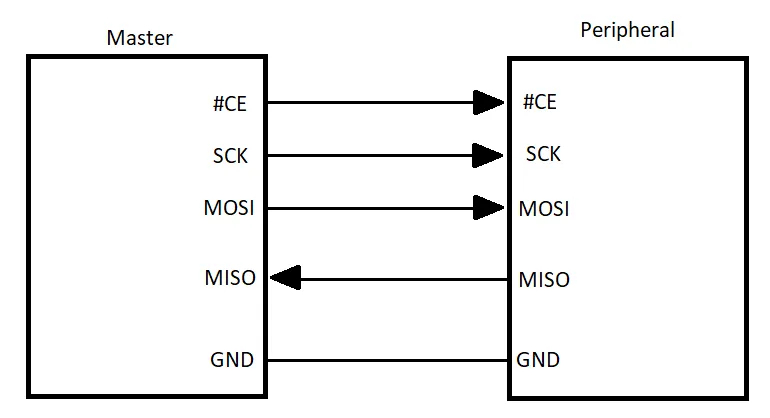
The master is in control of the chip select (often denoted as #CS, /CS, or sometimes SS) line and the clock line which is denoted as SCK. When a peripheral’s chip select line is pulled low, it will listen for and respond to commands from the master device, in the case of flash memory, these may be read or write commands along with addresses and the data to be written. The master can only communicate with one device at a time otherwise there is a risk of bus contention as multiple devices try to communicate at once.
The timing diagram below shows a typical sequence of sending data to a peripheral device. The communication is initiated by a high to low transition on the #CS line (this line must also stay low for the duration of the transmission). Commands are sent to the peripheral on the MOSI (Master Out, Slave In) line, each bit is transmitted with a transition on the SCK line. Data is read out from the peripheral on the MISO (Master In, Slave Out) line, again data is read at each transition of the SCK line.
SPI can be run in one of 4 modes determined by the value of two bits: the CPOL or Clock Polarity bit and the CPHA or Clock Phase bit. The mode must be determined beforehand and agreed by both devices and not all peripheral devices are capable of operating in all the modes. Most common is mode zero or mode three, where both bits are one or both bits are zero.
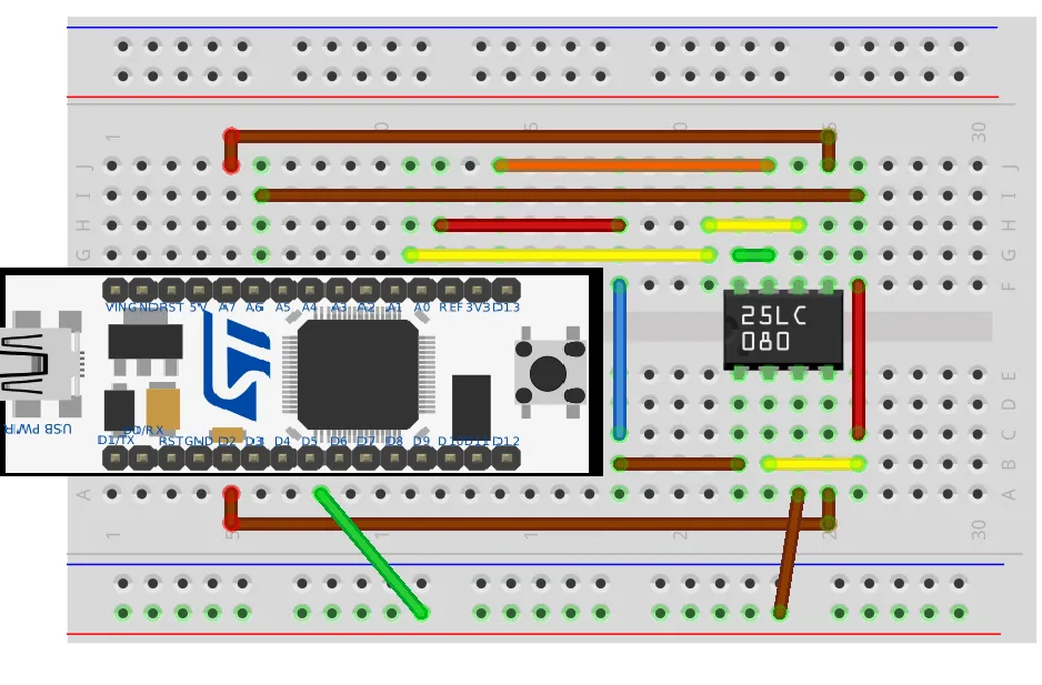
Capturing The Password
If you have the challenge device from the conference, the way it works is to read the password from flash memory upon boot. What this means is we can use a logic analyser to capture the communication as the device boots up and determine the password as it is read from flash. Once we understand how it obtains the password, we could write our own password to the flash chip and have the device read that upon boot.
To capture the communication, you will need to hook up the logic analyser pins to the pins of the flash chip (as well as a GND connection). When I do this, I tend to use channel 0 for #CS, channel 1 for SCK and then channel 2 and 3 for MOSI and MISO. Look at the datasheet for the flash chip to determine the pinout. If you are unsure of the pinout of a particular target, you can simply connect to all the pins and capture some data. From there you will probably be able to reverse engineer what the pins are doing. The #CS pin is fairly obvious as is the clock pin. It should be clear which pins are the data, but you may not know which is MISO and which is MOSI, however, you’ve now narrowed it down enough that it’s simple to just try either configuration and see what works.
Once you have connected the logic analyser wires to the target, fire up Sigrok Pulseview. It should find your Bitmagic probe and show you eight channels. If there is a problem connecting to the device, you may need to disconnect the Nucleo board from the computer and connect the Bitmagic probe again. Once Pulseview has identified the probe, it is usually fine to plug the target device back into USB (you may find its COM port has changed though).
In order to capture the data efficiently, we need to perform a little bit of setup in Pulseview. The first thing I do (and this step is optional) is to remove the unused channels to make the display a bit cleaner. Click on “channels” and deselect the ones we don’t need (everything from channel 4-8).

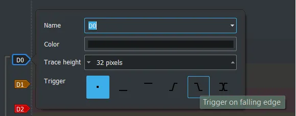
Next, set the trigger to falling edge (the line which goes down) on the #CS line.
This will mean we can start a capture, but it won’t actually capture any data until it sees a transition on the chip select line. Finally, make sure that the speed is fast enough, I normally use about 1-4MHz and set the number of samples to ~100K. If you mouse over the number of samples, it will tell you how long it will capture for, the communication will happen quite quickly, but you will probably want to capture a minimum of ~10mS. When determining the capture rate, you will need to set it to something at least twice as fast as the data rate, ideally you want it to be a minimum of four times the data rate. This will prevent aliasing of the signal and losing data. Usually, it is fine to just set it as fast as possible but you may get limited by the USB bus speed at some point so you don’t want to push it too far or it may fail to capture.
Once you have everything setup, start a capture, by clicking “run” and reset the device by pushing the button. Pulseview should have captured some data but at the moment we don’t know what it is.
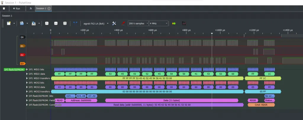
Most logic analyser software (Pulseview included) will have protocol decoders built in which will be able to decode the data you capture. Click on “add protocol decoder” on the top bar and search for flash (you can add a generic SPI decoder, but the flash decoder will tell you more about the commands being executed). Double click “SPI flash/EEPROM” and on the new channel which has appeared, click on the name on the left. This will bring up the configuration where we can tell the decoder which channel corresponds to which line of the SPI protocol. Set the CS, SCK, MOSI and MISO as per your connections. The software should now decode the data and will tell that a “read” command was issued and will show what data was returned. If it shows the data as hex, you can set it to display ascii in the dropdown where you configured the channels.
At this point, you should have the password. Enter it into the Serial console and see if it unlocks!
JTAG
First, a quick history lesson as to what JTAG is and why it came about. As electronic devices began to get more complicated and the components became more miniaturised, designers were able to fit more components onto a single PCB and those components were becoming more difficult to program and debug. Bad solder joints were common issues on these devices and could be difficult to track down.
The solution was to create a standardised way of debugging and programming devices from different vendors which may all be on the same PCB using a single interface. The Joint Test Action Group (JTAG) was created as a collaboration between several large vendors who determined the standard.
In order for a device to be compliant, it must implement the BYPASS and IDCODE commands. This ensures that devices in the chain can be identified and can be put into a mode where they do not respond to JTAG commands. This allows other devices in the chain to be debugged without interference.
As alluded to, JTAG devices are joined together in a chain, where the data output of one goes into the data input of the next device in the chain. The data out of the last device in the chain goes back to the programmer. The point where the programmer is connected to the chain is known as the Test Action Port or TAP and is technically what people mean when they say “JTAG Port”.
Connecting To Your Target
The STM Nucleo board (The white PCB on the breadboard) has a built in JTAG debugger called an ST-Link (Specifically an ST-Link V2) and this can be used to debug the processor which is running the challenge. Luckily for us, this is all connected correctly already so all we need to do is connect the board via USB and run some software to interface with the ST-Link.
The software we will use to interface with the ST-Link is called OpenOCD, this is essentially our bridge between the physical ST-Link debugger, and GDB. Open a terminal and move to the OpenOCD directory. Then, run the following command to start OpenOCD:
OpenOCD needs two configuration files in order to successfully connect to and control the target. One describing the interface, in this case, an ST-Link V2, and one describing the target, in our case, an STM32G0. The contents of these file could be concatenated together and provided as a single file but it’s common to simply provide two config files on the command line.
If OpenOCD successfully connects to the target, you should see something like the following output:
The last line of this output is the most important, if everything went well you should see that OpenOCD is listening for connections from GDB on port 3333.
Leave this terminal open (OpenOCD needs to remain running) but you can minimise it if you like. Open another terminal and navigate to the folder containing arm-none-eabi-gdb.exe.
Once connected, gdb will halt the target wherever it was executing which will likely be an unknown address. At this point, gdb has no idea what it is debugging so we need to tell it. Normally, at this point in the process you will have already dumped the firmware and performed some reverse engineering. So once you get to the point of debugging over JTAG, you know where the interesting functions are and you have some idea about how you want to proceed. In our case, I have provided an .elf file which is a binary file containing the code running on the device along with symbols as well as source code embedded into the file. This will make debugging much easier for the purposes of this workshop because we can skip the part where we need to reverse engineer the application.
To perform the next part of the workshop you will need to download the ELF file which contains the application code and symbols. The link is found here Hardware_workshop.elf.
Hopefully this has given you a bit of an introduction to the various ways you might go about attacking a piece of hardware, as with all vulnerability research, the key is usually to gain as much of an understanding about the target device as possible. This gives you the best opportunity for finding ways to subvert its operation.
Project Files
If you do not have the challenge programmed to the nucleo board, I have provided the STM32CubeIDE project below. This is the complete source code so you can make changes and play around to your heart’s content. If you do have the challenge already programmed on your device (i.e. you were at one of the workshops on the day) then this version is slightly updated compared to the version running on your device. I would recommend getting the STM Cube IDE because it includes (almost) all the tools you need to build and flash the device. You may find that the reset button does not work correctly though and this can be fixed by downloading the ST-Link Utility (sometimes called CubeProgrammer). Using this utility, you can change the “option bytes” (Target->Option bytes or alternatively ctrl-B) on the Nucleo and change “NRST_MODE” from “GPIO” to “Reset input only”.
The Project file can be found here: Hardware Workshop.zip
